
As semiconductor manufacturing expands across the United States, one challenge continues to shadow the industry's growth: finding workers with the specialized skills needed to enter the field.
At UC Santa Barbara, Demis D. John saw that challenge up close. As process group manager at the UCSB Nanofabrication Facility, he worked regularly with local semiconductor startups and industry partners, many of whom raised the same concern: they needed employees with practical cleanroom experience, but many students did not know those careers paths existed.
"We kept hearing the same thing from companies," John said. "They needed people with practical semiconductor skills, but many students didn't even know these careers existed."
Rather than viewing the workforce shortage as an industry problem alone, John saw it as an educational disconnect. Goleta and Santa Barbara area is home to a thriving semiconductor ecosystem, yet many local students were unaware of the opportunities available just beyond their classrooms.
Determined to bridge that gap, John joined forces with industry leaders and workforce-development partners, including Santa Barbara City College (SBCC) dean, Jens-Uwe Kuhn, to explore solutions. Their efforts coincided with discussions led by the Santa Barbara South Coast Chamber of Commerce's Manufacturing and Technology Committee, where workforce development has consistently emerged as one of the region's most urgent needs.
Those conversations led to the creation of UCSB's Cleanroom Bootcamp, a one-week immersive training program recognized by the Institute of Electrical and Electronics Engineers (IEEE), the world's largest not-for-profit technical professional organization. Supported by the National Science Foundation Advanced Technological Education grant awarded in 2021, and adapted from the training model developed by Professor Matthias W. Pleil at the University of New Mexico, the program addresses the specific workforce needs of Santa Barbara's rapidly growing semiconductor industry.
Central to the bootcamp is a powerful idea: remove barriers to access. Rather than expecting community colleges to shoulder the burden of building expensive semiconductor facilities, the model offers students access to UCSB's world-class nanofabrication cleanroom and its industry-grade equipment.
Today, the bootcamp serves as a gateway to semiconductor careers, introducing participants to cleanroom operations and foundational manufacturing processes. A comprehensive implementation handbook supports colleges and universities nationwide in replicating the model.
John played a leading role in developing one of the program's most distinctive features: IEEE Micro-Credentials. Created through a collaboration among UCSB, University of Southern California, and the California Defense Ready Electronics and Microdevices Superhub (CA DREAMS) Microelectronics Hub, the credentials provide industry-recognized validation of specific technical skills.
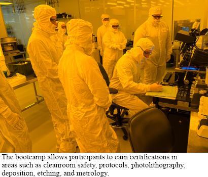
Unlike traditional degrees, the micro-credentials are modular and stackable, allowing participants to earn certifications in areas such as cleanroom safety, cleanroom protocols, photolithography, deposition, etching, and metrology.
"The goal was to create credentials that industry immediately understands," John said. "When employers see those credentials, they know a candidate has demonstrated specific skills and represents a lower-risk hire."
Forty-two participants have earned certifications since IEEE officially approved the micro-credentials for the bootcamp in August 2024.
The program's reach extends beyond university and college students. Participants also include faculty members, employees seeking to upskill, professionals transitioning into new careers, and educators trying to bring semiconductor training back to their own institutions.
Joey Vo, a lab-operation engineer from the University of Southern California Nanofabrication Lab, enrolled in the bootcamp to experience how UCSB was preparing the next generation of semiconductor talent.
"My university was seeking to learn about the course at UCSB so that we can create the course here for our users," Vo said.
For SBCC student Jennifer de Prada, the program brought a shift in her career. She entered the bootcamp while pursuing an associate degree in computer science.
"While I truly enjoyed programming, I found myself even more interested in learning what happens at a deeper hardware level and how the technology we use every day works at its core,” she said.
The hands-on experience in the cleanroom exposed de Prada to a career path she had not previously considered. “The cleanroom training at UCSB gave me a strong introduction to how the semiconductor industry operates and helped me realize the educational path I want to pursue. Thanks to this experience, I was able to secure a full-time position in one of the cleanrooms at Teledyne FLIR,” she added.
What began as a response to a local workforce challenge has grown into a scalable model for semiconductor education. Through internships, cleanroom bootcamps, advanced microfabrication training, and a “train-the-trainer” model designed to be replicated nationwide, the UCSB Nanofabrication Facility is helping build pathways into one of the country's most critical industries.

Demis D. John, Process Group Manager at the UCSB Nanofabrication Facility, showcasing a silicon wafer.