
It seems straightforward enough: materials are combined according to a precise recipe to make a semiconductor light-emitting diode (LED), a current is run through it, and light is emitted. But it’s not as simple as that, mainly because it is extremely difficult to achieve high levels of efficiency in converting electricity to light in an LED. That key parameter of performance has two main components: internal quantum efficiency (IQE), which refers to how effectively electron energy is transformed into photons inside the material; and light-extraction efficiency (LEE), the percentage of photons emitted inside the LED material that make it to the outside.
Lacking specific architecture, in any LED made of any material and emitting light at any wavelength, only around ten percent of the photons generated within the semiconductor are emitted as visible light. The rest remain trapped due to a refraction phenomenon that can cause the photons to bounce back and forth repeatedly within the LED until the energy is dissipated through one of several mechanisms. The semiconductor boundaries must be engineered to release light to the outside. Liberating the light generated in LEDs has been the life’s work of Claus Weisbuch, a permanent part-time faculty member who came to UCSB as part of a Regents Professors program in 2002.
As of 2017, Weisbuch had spent 25 years — 15 at UCSB — working to increase the light-extraction efficiency of LEDs. He spent the early part of his career studying the physics and performance of semiconductor materials, and his 1991 book on the subject, Quantum Semiconductor Structures, became a widely used university text. While at Bell Labs from 1979-81, he explained the theory of light emission from quantum wells in semiconductor-based optical devices.
In the late 1990s, thanks to the breakthrough work of fellow researcher and SSLEEC co-director Shuji Nakamura, the IQE of blue LEDs was high, but LEE was 20 percent at best, so only one in five photons generated in the semiconductor material was being emitted as light.
At UCSB, Weisbuch worked to improve LEE by addressing the fact that photons bouncing around in the quantum well of a semiconductor can escape as visible light only by following certain angles of refraction. He developed various techniques to ensure that photons traveled in the right direction.
“Photonic micro-cavities” and “photonic crystals” were two early approaches. Later, he performed the mathematical modeling for “roughening,” which involved etching away a sapphire substrate to pattern the gallium nitride (GaN) layer, causing more photons emitted from the quantum well to be refracted at desirable angles. But roughening was complicated and time-consuming and was eventually replaced by the currently used process, called “pattern sapphire substrate,” for which Weisbuch also did modeling work. In that approach, the LED’s sapphire substrate is patterned with bumps, and then the GaN layer is added. The textured substrate ensures that photons emitted from the quantum well in a direction that does not allow them to escape are refracted at an angle more likely to result in their being extracted on their next attempt to exit the LED.
Weisbuch then turned to addressing efficiency “droop,” which refers to the fact that IQE decreases as the current to an LED increases. The physical mechanism at work had long been debated, especially in the absence of direct evidence proving its existence. Working with Jim Speck, as well as with colleagues at Ecole Polytechnique in France, his base when not at UCSB, Weisbuch devised an experiment that made it possible to observe “hot electrons” and prove the existence of the droop mechanism.
Having significantly increased understanding of blue-LED performance and its limits, in 2017 Speck and Weisbuch received funding to do the same for green LEDs, which were only about 40-percent efficient at that time, compared with today’s 80-plus-percent-efficient blue LEDs at low currents. The disparity results from the fact that to emit green light, the semiconductor has to contain a higher percentage of indium, which causes many imperfections in the crystals and fluctuations in material composition. Speck and Weisbuch are also seeking new semiconductor structures to address another challenge, which is that higher indium content required for green light, relative to blue light, produces more powerful internal electric fields, which, in turn, diminish the recombination rate of electrons and holes so that fewer photons are generated.
“We have the challenge of modeling the electronic and photonic activities, diminishing the electric fields, and then putting those two things together to optimize the structures,” Weisbuch says. “It’s quite complicated but very exciting.”
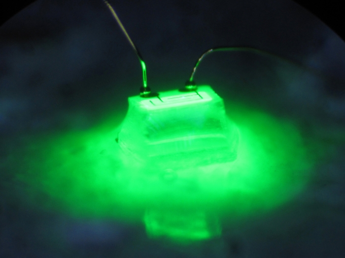
A green LED fabricated on patterned sapphire